|
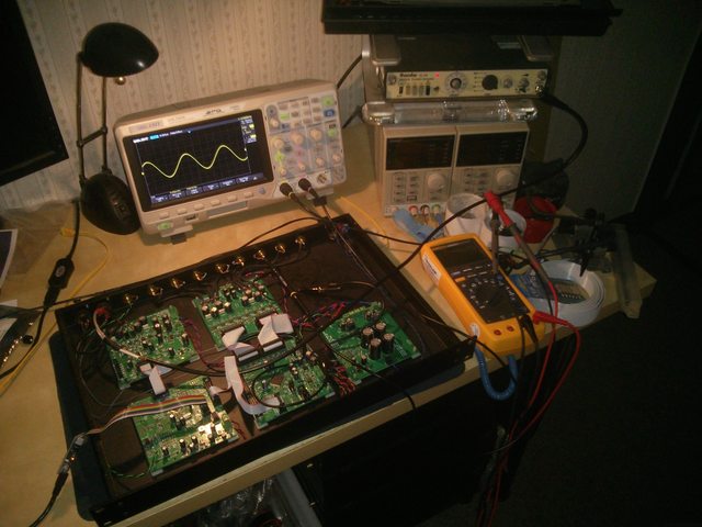
So my 2 input (XLR) 8 output (phono/RCA) box had been giving me some worries over the past couple of months, and in fact I gave up on it for a few weeks, But I plugged it all back in last night and... it just works.
Stupidity was the main cause for issue. My output phono sockets on the back actually are ordered as "4 5 6 7 0 1 2 3" to match up with the Sigma Studio output channels. As the ribbon connectors on the buffer PCB and DAC PCB are aligned in the same orientation to the edges of the PCB, when they are put together they are "opposite" and the ribbon cable has to twist 180 degrees to fit. Pretty dumb not to notice it but there we are, humanities flaws being shown in their finest hour. Simple waveform generator (ancient noisy thing) on the Right channel XLR input, mapped to channel 1 output. And it works (and it works with any other channel combo as well). Nothing special but it's a start, adding crossovers in is just done in the DSP now. Although it won't boot from the EEPROM at the moment, assume I actually put an EEPROM chip in the socket.... maybe I should go check that.... Oh and my maximum output from the buffer board with the dac at 0dB output is 5Vpp, so I need to change a few resistors on the buffer board or some amps will get fried.
0 Comments
The DAC chip I have been using, the ADAU1966, no longer seems to be stocked in Farnell. There is also a new variant the ADAU1966A which looks compatible, and there is some limited stock at Digikey/Mouser. RS have stock of the ADAU1966 but the price is much higher (over double) than I last paid for a few. Both parts are shown as production parts so unsure what has changed.
Cirrus Logic offer a range of 8 Channel DACs that support TDM data modes. They have less channels than the ADAU1966, but may be usable. I need to check master clock requirements and other details but will need a new design. They also seem to be in stock at a number of places. Reworking PCB redesigns and unraveling all the interwoven tracking and component placement without destroying the whole design is hard. Sometimes it is just easier to start again!
As I have been reviewing all the designs I have slowly been making lots of small changes, and lots of small changes leads to lots of PCB rework. This is fine but I am becoming more and more busy with life these days so it will take some time. And in fact just starting from scratch on several PCB layouts may be quicker than trying to work out what I did last time. Also now looking at ADC options. The TI PCM4202 is a nice spec ADC chip but seems to have fragile I/O pins. One wrong setting or connection on the I2S interface can cause permanent damage. It would be good to have something a little more robust in it's place. Again this would be another new PCB layout, or several if other revisions are needed to fix any issues. We will get there eventually! |
Paul JanickiAn electronics engineer and a long term electronics hobbyist. I like tinkering with stuff and making things. Archives
July 2022
Categories |

 RSS Feed
